Week - 8: Electronics Design
Week 8 of the Electronics Production course includes:
Group Assignment:
- Use the test equipment in your lab to observe the operation of a microcontroller circuit board.
- Send a PCB out to a board house.
Individual Assignment:
- Use an EDA tool to design a development board that can interact and communicate with an embedded microcontroller.
- Produce and test the board.
Extra Credit Opportunities:
- Try another design workflow.
- Design a case for the board.
- Simulate the board's operation.
PCB Design with KiCAD 
I have followed the KiCAD tutorial available at: KiCAD 7.0 Tutorial . Below are my shorter version of the basic steps for the PCB design.
The typical workflow in KiCad consists of two main tasks: drawing a schematic and laying out a circuit board. A KiCad project is a folder with a project file, a schematic, a board layout, and optionally other associated files such as symbol and footprint libraries, simulation data, purchasing information, etc.
- Typically, the schematic is drawn first.
- When the schematic is complete and the design has passed an electrical rules check (ERC), the design information in the schematic is transferred to the board editor and layout begins. Often the schematic will need to be updated after layout has begun.
- Laying out a circuit board.
- When the board layout is complete and the board has passed the Design Rules Check (DRC), fabrication outputs are generated so that the board can be manufactured by a PCB fabricator.
Design
I'll be designing a development board using SAMD11.
KiCad
KiCad is an open-source EDA software suite for designing PCBs and schematics. The typical workflow in KiCad involves two primary tasks: drawing a schematic and laying out a circuit board. A KiCad project encompasses various files within a folder, including a project file, schematic, board layout, and potentially other associated files like symbol and footprint libraries, simulation data, and purchasing information.
The process begins with creating a schematic, where components are selected from libraries and connected using wires to represent electrical connections. After completing the schematic, an Electrical Rules Check (ERC) is performed to ensure the design's integrity. It's common for schematics to undergo revisions even after the board layout has begun, necessitating updates and iterations to maintain consistency.
Once the schematic is finalized and passes the ERC, the design is transferred to the board editor. Here, the netlist generated from the schematic is imported, and footprints for components are automatically placed on the board. Designers then arrange these components, taking into account factors like size, placement, and signal routing. Traces are drawn to establish electrical connections between components, adhering to design rules and constraints.
After laying out the board, a Design Rules Check (DRC) is performed to ensure compliance with manufacturing specifications. Any errors or warnings identified during this check are addressed to ensure manufacturability. The board layout undergoes thorough review to confirm alignment with design requirements before saving the final layout.
Once the board layout is complete and passes the DRC, fabrication outputs are generated.
.png)
To add components while designing there are a lot of libraries but for Fab Academy, there is a seperate library with all components. This avoids confusion since there are multiple libraries with same components.
.png)
Next step to follow these installation steps mentioned in the repository for correct access to the library while designing. So i followed those steps.
.png)
SAMD11
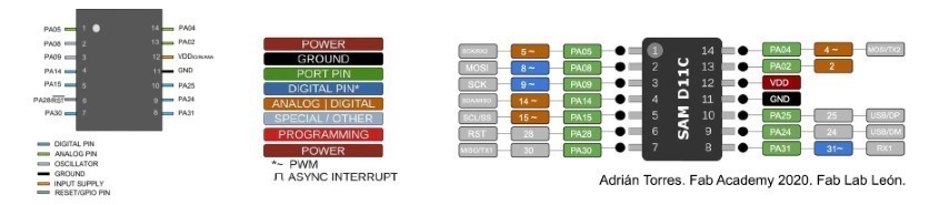
SAM D11 is a microcontroller developed by Microchip Technology. It belongs to the SAM D family of ARM Cortex-M0+ based microcontrollers. SAM D11 microcontrollers are known for their low power consumption, making them suitable for applications where energy efficiency is critical. They are commonly used in various embedded systems, IoT devices, consumer electronics, and other applications requiring low-power operation and moderate processing capabilities. SAM D11 microcontrollers typically feature a range of peripherals such as ADCs, UARTs, SPI, I2C, timers, and GPIOs, making them versatile for a wide array of applications.
For my development board, I'm using this microcontroller SAMD11. So I used this pin out diagram to understand the microcontroller and use it in my design accordingly.
Regulator circuit
SAMD11 runs on 3.3V but the laptop output voltage is 5 V. To regulate the voltage, I referred this design so my board would not damaged.

Here is the regulator circuit
.png)
Adding FabAcadmy Libraries for KiCAD 
Download the KiCAD library from Gitlab:
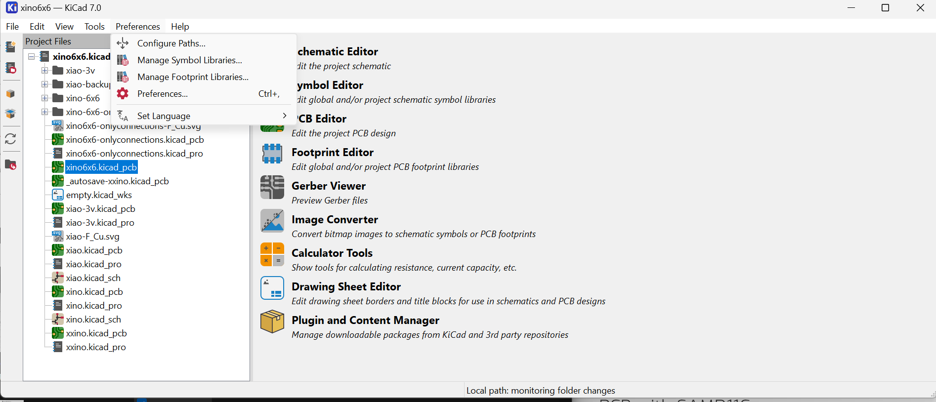
and follow readme.md file for instruction how to intall library. I copied the whole folder downloaded from gitlab to: C:\Program Files\KiCad\7.0\lib.
Remember to instal libraries when you open project (not in the schematic or pcb project file)!
I prepared the schematic design reviewing Samdino . I started preparing my first board design using KiCAD.
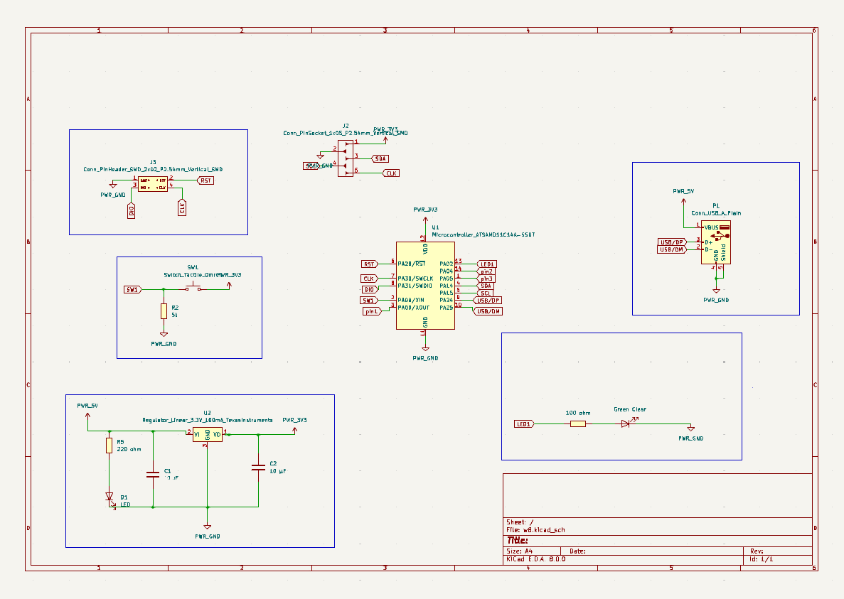
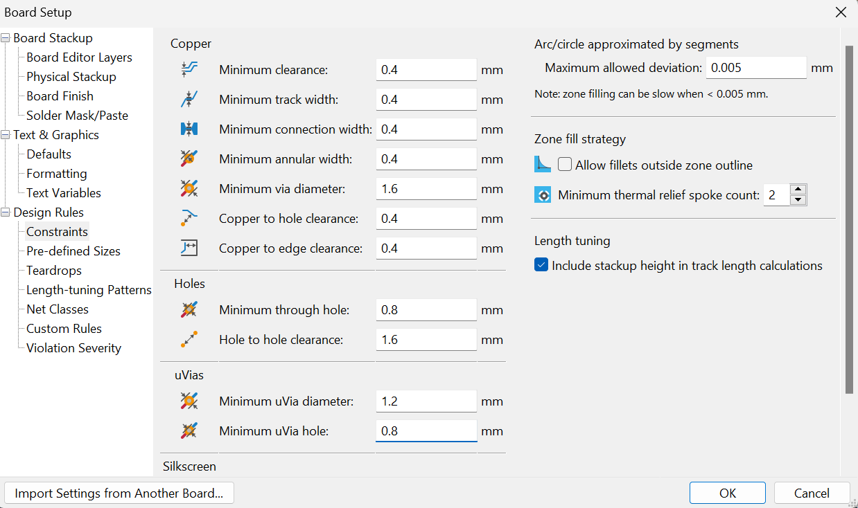
The design was prepared using default Design Rules and passed Design Rules Checker. The following parameters were shared by our instructor.
- Schematic design is done and next step is the design of PCB layout of the circuit. So I opened PCB editor.
.png)
The design of the board is presented below. I designed a compact board with the measurement of 32 mm X 40 mm. After 2 hours of routing, I had obtained the following result.
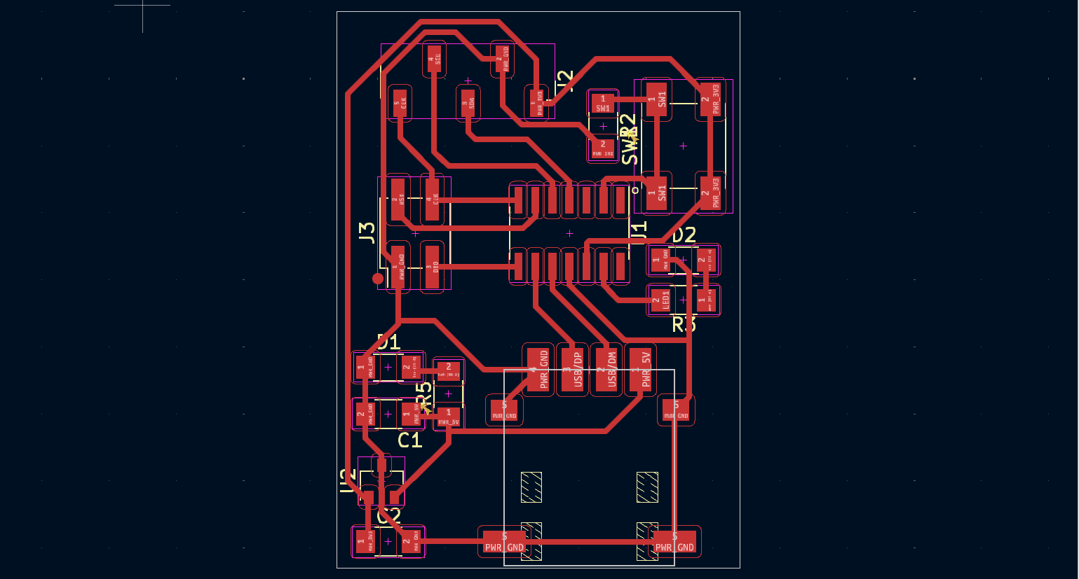
For integrating the C-type connector I used a proshplay board for which the footprint was shared with us by our instructor.
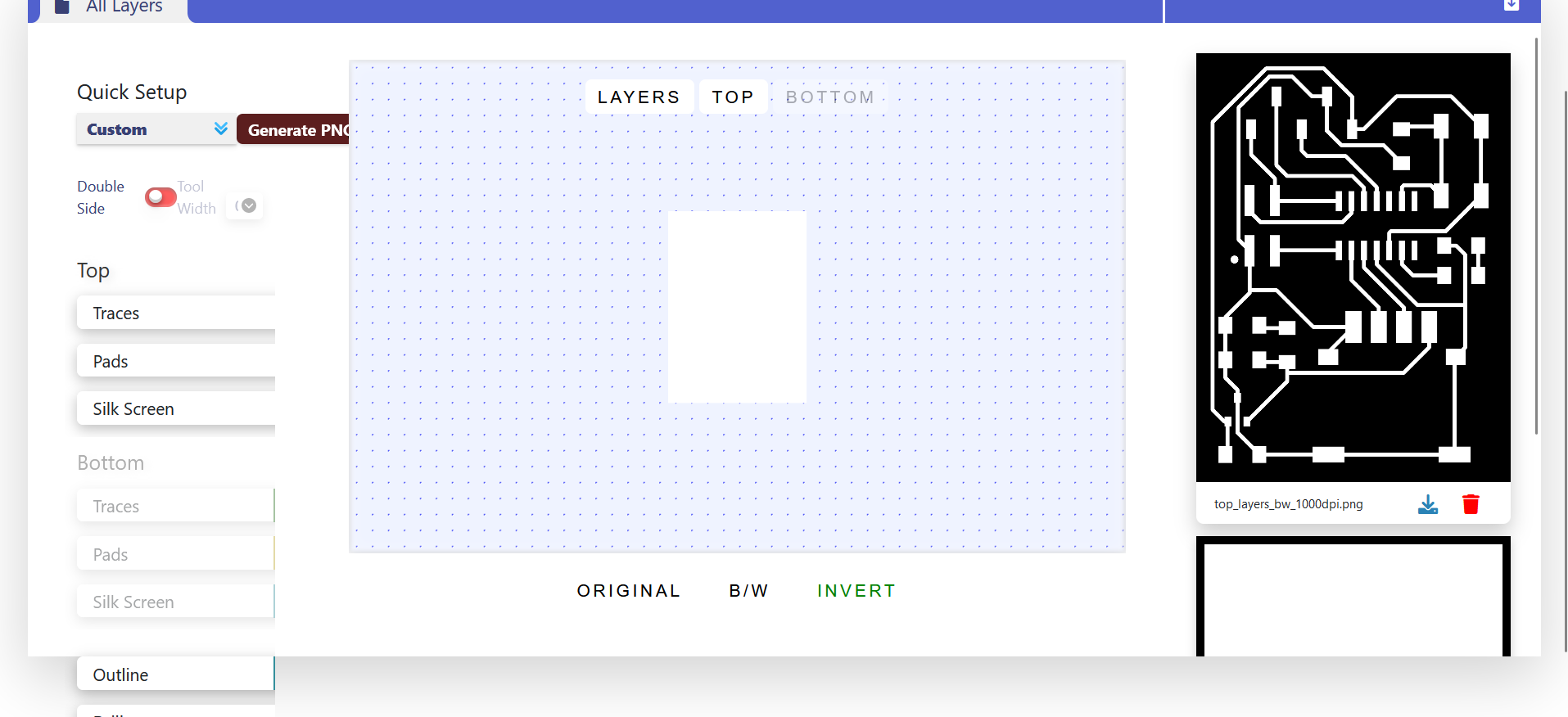
Gerber to PNG
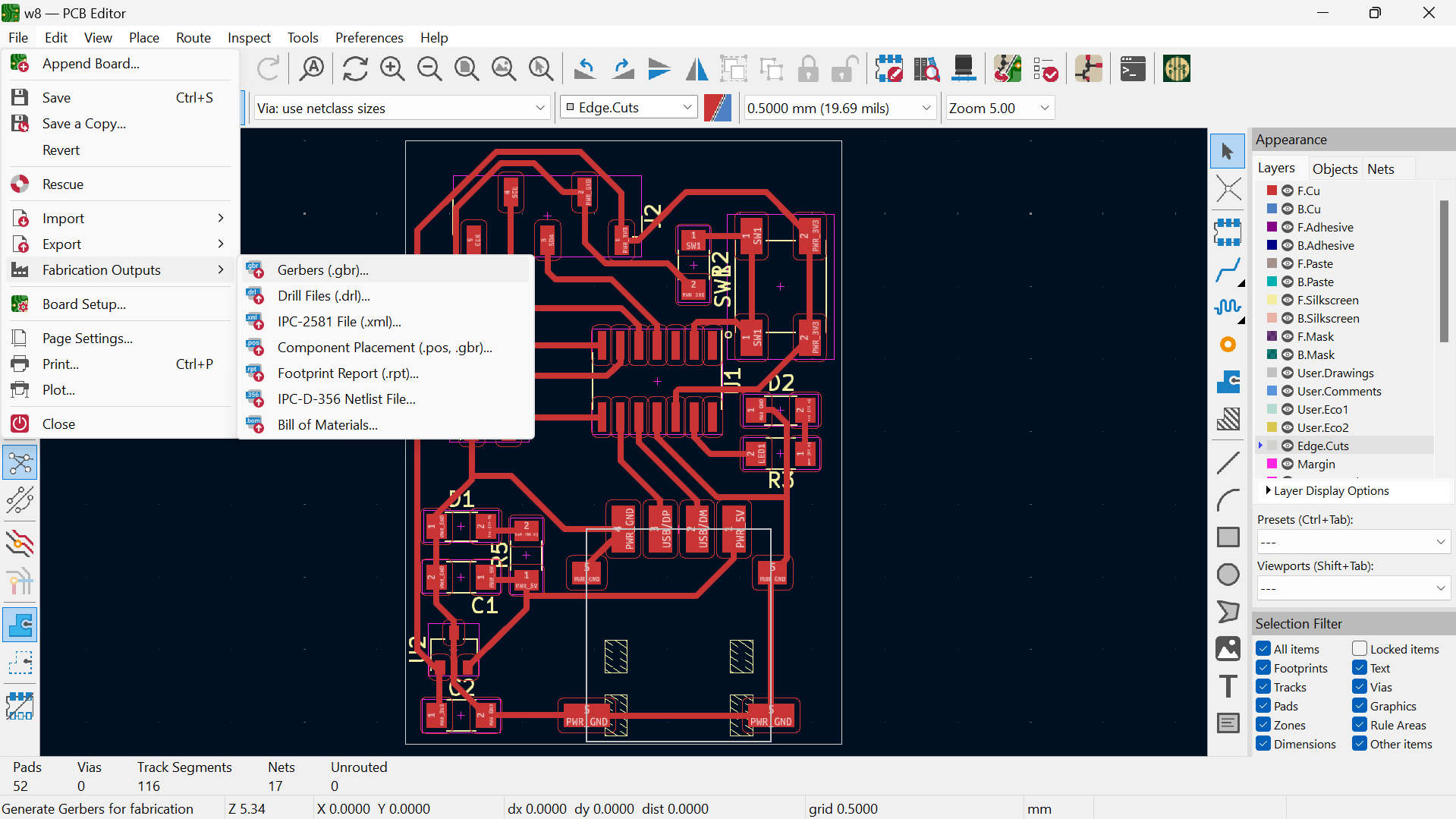
Next step is to export the Gerber file and convert it into PNG for milling. Our FabLab has a special website for this conversion. Visit this website.
- So first, I exported the gerber file from KiCad.
Super Fablab Kerala has designed a tool named Gerber to PNG which helps us to get a PNG file of traces and outline that can be milled using Roland MDX PCB Mill. Here’s a screenshot of the same.
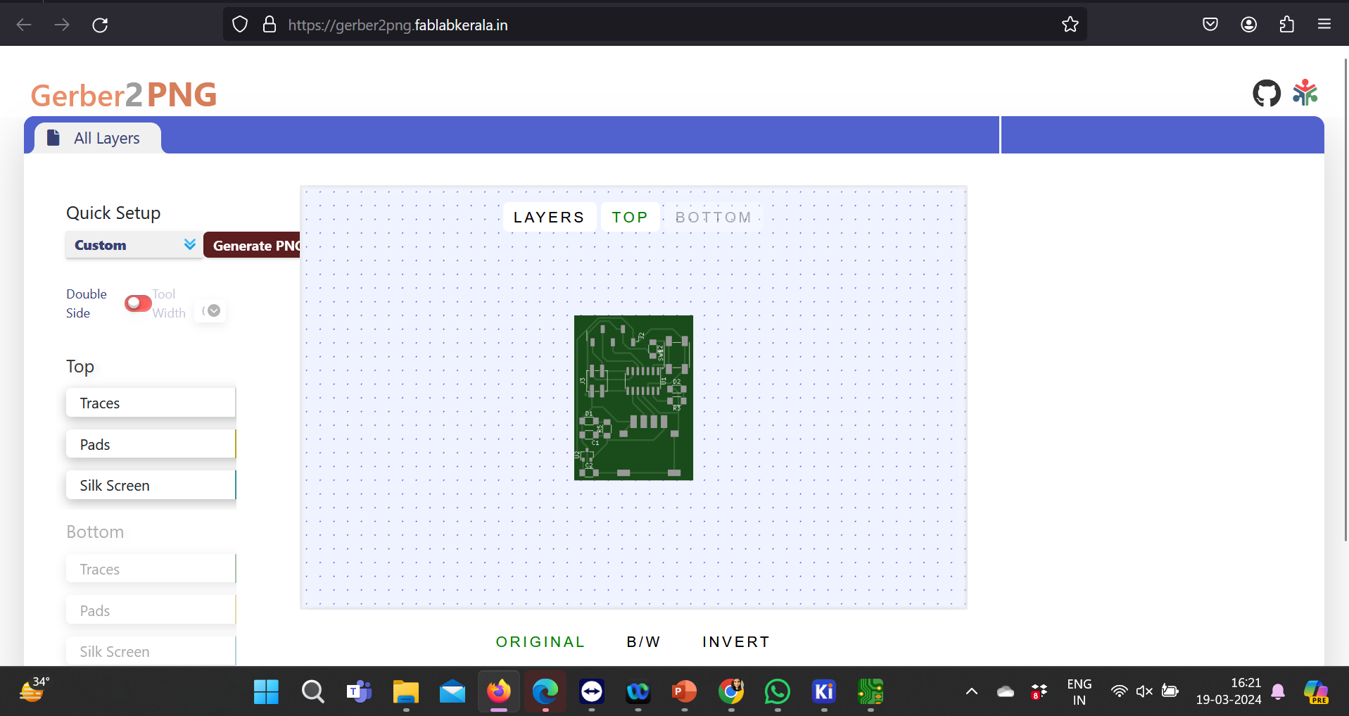
When the gerber files were uploaded, we got the png files for traces and outline as follows:
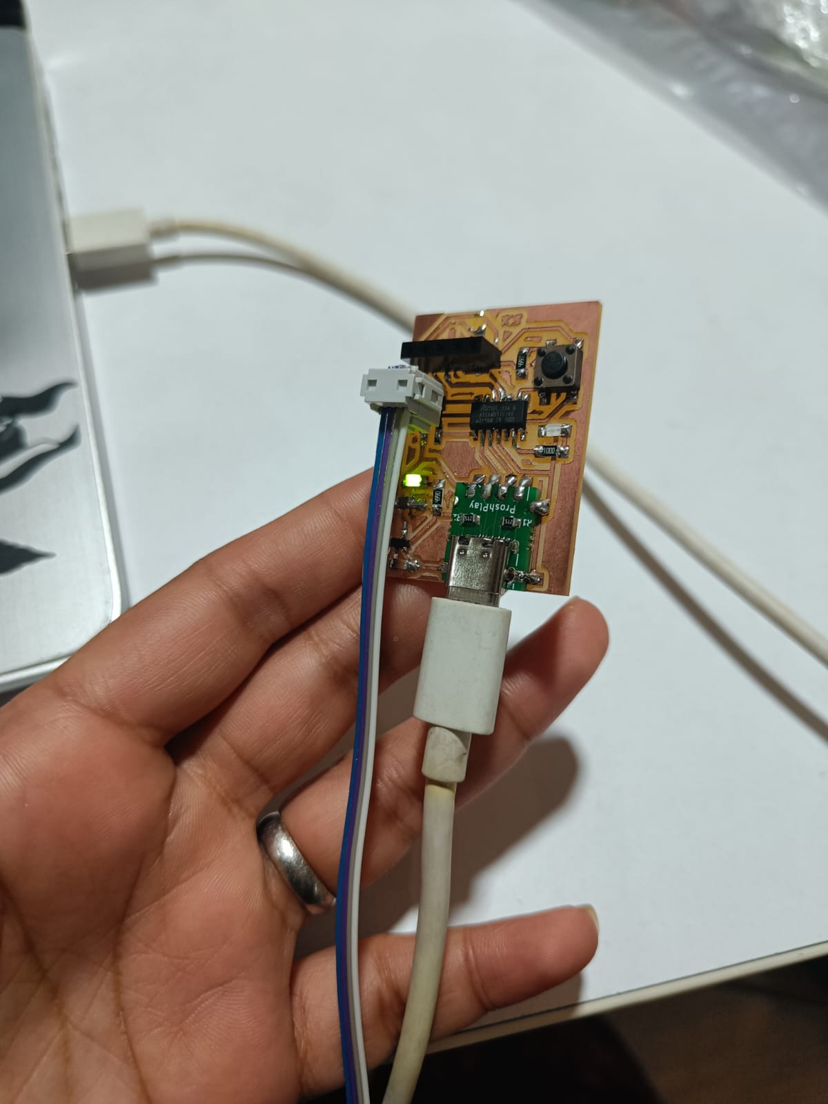
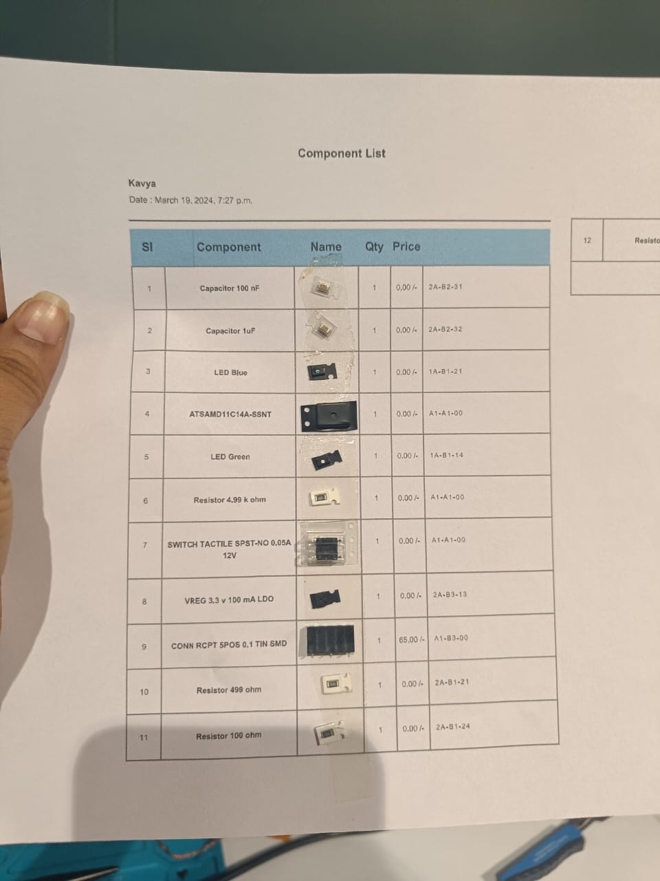
I milled my PCB and soldered all the components mentioned in the list.
Then I added the additional board manager board from this link following the steps. Once done I selected the following board and programmer and burnt the bootloader.
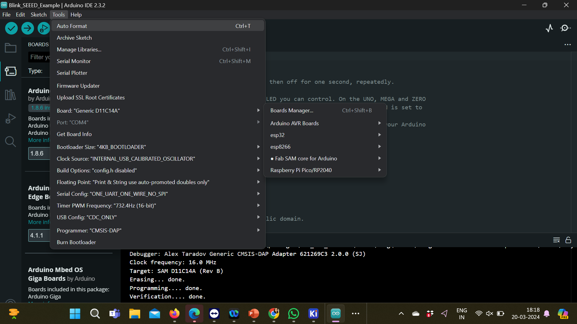
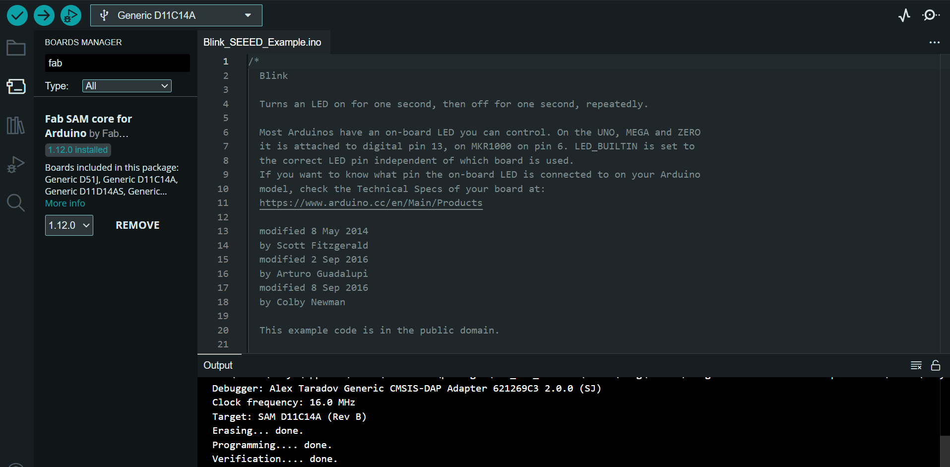
I am troubleshooting the board to load them for programs as the port is not getting displayed.
Programming
As we had programming in week six, I did the same workflow this time as well.
LED ON/OFF via button
    const int buttonPin = 2; // Button pin from SAMD11C14A
    const int ledPin = 4; // LED pin from SAMD11C14A
    int ledState = LOW; // Current LED state
    bool previousButtonState = HIGH; // Previous button state, assuming pull-up

    void setup() {
    pinMode(ledPin, OUTPUT); // Initialize LED pin as output
    pinMode(buttonPin, INPUT_PULLUP); // Initialize button pin as input with pull-up resistor
    }

    void loop() {
    bool currentButtonState = digitalRead(buttonPin);
    if (currentButtonState == LOW && previousButtonState == HIGH) {
        // Button was pressed
        ledState = !ledState; // Toggle the LED state
        digitalWrite(ledPin, ledState); // Set the LED to the new state
    }
    previousButtonState = currentButtonState; // Update the previous button state
    }
The code uploaded sucessfully!
.png)
I have fixed my board and loaded the following program to test the led blinking on my board.